The vision of Sanan IC is make "Everything Smart & Connected". Today, there are more than 50 billion IoT devices worldwide, and more devices will join IoT. The supply capacity of RF communication, optical communication, LiDAR and power conversion chips is far from being able to meet the needs of the world.
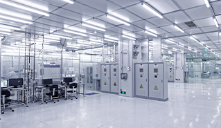
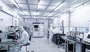
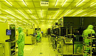
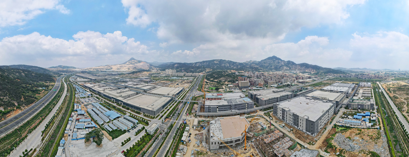
To make this vision come true, the world needs more large-scale compound semiconductor wafer foundries. At present, Sanan IC has deployed three large-scale wafer manufacturing factories in China, and with more than 20 years of experience in production management and quality management system, "Sanan IC Experience" can quickly be replicated globally.
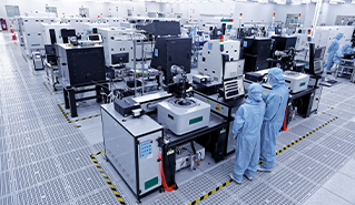
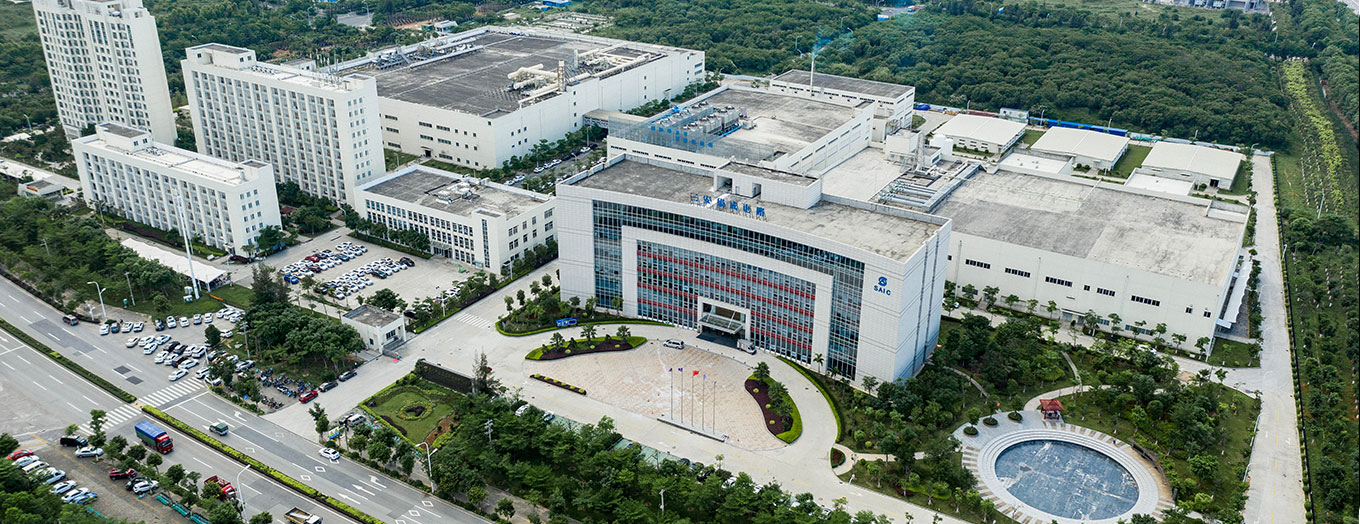
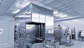
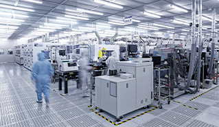
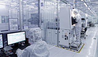
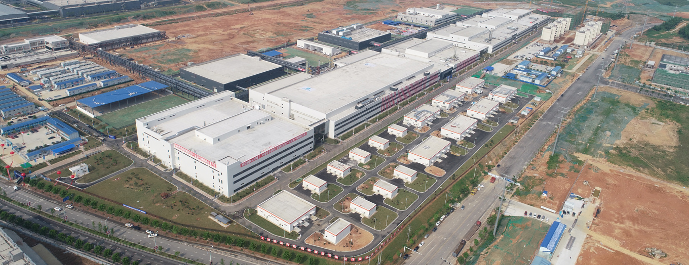
Sanan IC's first Mega Fab was built in Xiamen, Fujian in 2014. The factory covers an area of 180,000 square meters, with a total investment of approximately RMB 4.5 billion and a comprehensive monthly production capacity of 30,000 wafers. As the headquarters and R&D center, it has gathered global elites in compound semiconductor R&D and manufacturing, and deployed R&D laboratories and production lines, covering four major sectors including microwave VVF, power electronics, optical communications, and filters.
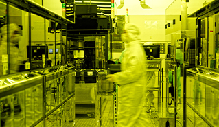
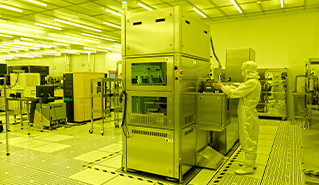
In 2017, the second Mega Fab was built in Quanzhou, Fujian, with a total investment of approximately RMB 33.3 billion, covering an area of over 1,500,000 square meters, equipped with vertically integrated production lines for Gallium Arsenide (GaAs) and filters, with a comprehensive monthly production capacity of up to 8,000 GaAs wafers, 128Mu filters, providing abundant VF front-end chip and optical communication chip production capacity for the communication industry. In 2020, the construction of the third Mega Fab began in Changsha, Hunan, with a total investment of about RMB 16 billion, covering an area of over 660,000 square meters and a comprehensive annual production capacity of 400,000 wafers. It builds vertically integrated production lines for Silicon Carbide (SiC) and Gallium Nitride (GaN) , covering substrate materials, epitaxial growth, chip manufacturing, packaging, testing and other sections, which will accelerate the popularization and iteration of Wide Band Gap semiconductor power devices.
Established: May, 2014
Investment: $7.85M
Area: 180,000㎡
Capacity: 30,000 Wfr/Mo

Established: Dec. 2017
Investment: $4.6B
Area: 1,500,000㎡
Capacity: 8000 GaAs Wfr and 128Mu ea/Mo
Established: Jun. 2021
Investment: $2.3B
Area: 660,000㎡
Capacity: 30,000 Wfr/Mo